Add to Cart
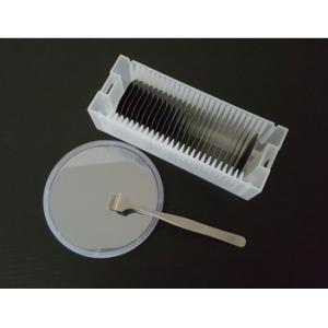
2inch N-type P-type thickness 350um primary grade Dummy grade Indium Phosphide crystal InP substrates wafer for LD
Indium phosphide single crystal material is one of most important semiconductor compound, which is key raw material for laser diode of indium phosphide substrate(LD), light emitting diode(LED), photodetector in optical communication production. Those parts play information launching, transmitting, amplifying, reception function .
Indium phosphide is ideal for high-frequency devices, as HEMT, HBT and so on.Because of its great property, it is widely used in fibre-optical communication, microwave, millietric wave, anti-radiation of solar cells, heterojunction transistor, other similar advanced technology and so on. Main production methods of indium phosphide single cryatal material include LEC, improved LEC, VCZ/PC-LEC, VGF, VB and so on.
Specification
| Item | Diameter | Type | carrying concentration | Mobility | Resistivity | MPD |
| S-InP | 2 | N | (0.8-6)X10^18 | (1.5-3.5)x10^3 | <500 | |
| 3 | <500 | |||||
| 4 | <1x10^3 | |||||
| Fe-InP | 2/3/4 | SI | >1000 | >0.5x10^7 | >5x10^3 | |
| Zn-InP | 2/3/4 | P | (0.6-6)X10^18 | 50-70 | <1x10^3 | |
| No dope InP | 2 | N | <3x10^16 | (3.5-4)x10^3 | <5x10^3 | |
| Other | ||||||
| Orientation | (100)/(111)±0.5° | Flatness | ||||
| TTV | Bow | Warp | ||||
| <12um | <12um | ≤15um | ||||
| 1st OF Flat | 16±2mm | 22±2mm | 32.5±2.5mm | |||
| 2st OF Flat | 8±1mm | 11±2mm | 32.5±2.5mm | |||
| Surface:1sp or 2sp ,2inch 350±25um,3inch 600±25um,4inch 625±25um,or by customized | ||||||
sample

Why choose us— ZMKJ .?
Dealing Term
Delivery Time: 10-25 days
Shipping term: Exw factory, FOB Shanghai
Delivery term: Express service/Air freight
Payment term: T/T 100% in advance, or Deposit on order
As Optics mostly are small size, delivery we prefer to use Express.
It will be highly appreciate if you can provide Express account for delivery, thanks for supports!